Realizing scalable quantum photonic networks requires precise, dynamically tunable control over light–matter interactions at subwavelength scales. This capability is currently bottlenecked by the static nature of conventional planar metamaterials, which limits real-time quantum state routing. This work introduces a dynamically reconfigurable planar metamaterial platform featuring an atomically thin graphene monolayer to achieve deterministic, continuous tuning of quantum emitter coupling environments. By exploiting transition boundary conditions in rigorous full-wave finite element simulations using COMSOL Multiphysics Software, we map the evolution of highly localized near-field resonant modes, identifying a dominant localized surface plasmon resonance at 4.3 THz. We demonstrate that actively modulating the graphene chemical potential (Ef) from 0.05 eV to 0.6 eV provides external control over the Local Density of Optical States (LDOS). This control enables a transition from weak uncoupled states to a near-perfect critically coupled light-matter absorption regime (98%). Crucially, the spatial field distribution transitions from an edge-confined mode to a symmetric multi-polar profile at 5 THz, culminating in a complete spatial mode inversion at 6 THz. This framework provides the missing design rules for actively steering complex quantum states, establishing a concrete pathway for fully integrated, dynamically programmable quantum photonic circuits.
The generation, routing, and control of complex quantum states—such as single-photon states, squeezed light, and entangled photons—are foundational to quantum computing, secure quantum key distribution, and high-precision quantum metrology by 1. Traditional quantum optical setups rely on bulky crystals or high-quality-factor conventional cavities to enhance light-matter interactions observed by 2. However, these approaches face severe challenges regarding scalability, physical footprint, and rigid operating bandwidths that hinder real-time quantum state routing 3.
Planar metamaterials have emerged as a disruptive paradigm to overcome these limitations. By engineering subwavelength-scaled, artificially patterned structures (meta-atoms), researchers can manipulate the phase, amplitude, and quantum vacuum fluctuations of light at will like the case of 4. When combined with two-dimensional (2D) materials like graphene, these planar platforms gain crucial dynamic tunability and high field confinement, making them ideal for manipulating light-matter interactions at the single-quantum limit as seen by 5.
Despite these advances, a critical bottleneck remains: current tunable metamaterial designs lack a scalable, continuous, and deterministic mechanism to dynamically control the coupling efficiency of quantum states 6. Most existing models rely on static geometries that cannot adapt to real-time quantum state routing or varying emitter frequencies 7. To address this gap, this study introduces a comprehensive, dynamically reconfigurable planar metamaterial framework optimized for deterministic quantum emitter coupling and light-matter interaction control.
Rather than treating the platform as a static system, we deploy a transition boundary condition to explicitly map how a 1 nm graphene monolayer continuously modulates the near-field quantum environment. Specifically, we reveal how actively tuning the graphene chemical potential from 0.05 to 0.6 eV serves as a direct external dial to control localized surface plasmon resonances near 4.3 THz, governing the local density of optical states (LDOS) 8. By evaluating the precise correlation between unit cell geometry, material response, and localized field enhancement, this work establishes the practical design rules required to build integrated, dynamically programmable quantum photonic circuits.
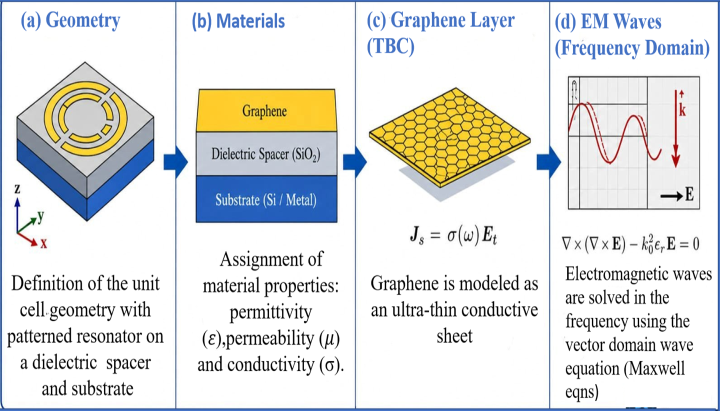
The computational and theoretical workflow engineered to model the quantum-cooperative planar metamaterial bridges geometric design, material characterization, boundary approximation, and full-wave electromagnetic solutions. The complete schematic sequence from unit cell layout to frequency domain quantum-field environment calculation is systematically detailed in Figure 1.

The design begins by defining the subwavelength unit cell geometry (Figure 1a) to optimize localized light-matter interactions. The meta-atom comprises a patterned concentric split-ring-like resonator configuration. This structure is patterned atop a dielectric spacer layer, which rests on a continuous substrate backbone. The structural stack consists of three functional regimes (Figure 1b): an active monolayer graphene sheet, a dielectric Silicon Dioxide ) spacer layer, and a Silicon metal substrate base. Each domain is mathematically is defined by assigning its constitutive parameters: frequency-dependent complex permittivity (
 ), permeability and (
 electrical conductivity (σ) which dictates the electronic backing of the quantum control interface.
Massive mesh counts caused by modeling an atom-thin layer of 1 nm in a macroscopic mesh are avoided by modeling graphene as an ultra-thin conductive sheet (Figure 1c). We implemented a Transition Boundary Condition (TBC)) 9, governed by the surface current density in equation (1):
 | (1) |
where  is the surface current density vector,
  represents the tangential component of the localized electric field of the interface.
The complex surface conductivity of the monolayer graphene sheet (σ(ω)) governs the light-matter coupling parameters and is modeled using the comprehensive Kubo formulation by 10. The complex conductivity is dictated by the summation of intraband electron-phonon scattering and interband electron-electron transitions 11, given by:
σ(ω)= σintra(ω)+ σinter(ω)(2)
The intraband scattering contribution is mathematically evaluated using:
 | (3) |
while the interband electron transition contribution is approximated via:
 | (4) |
where e is the is the elementary electron charge,  is the reduced plank constant
  is the Boltzmann constant,
  is the angular operating frequency, T is the active operating temperature (300 K),
  is the quantum periodic time (1x 10-13 s) and
  is the dynamically tuned chemical potential.
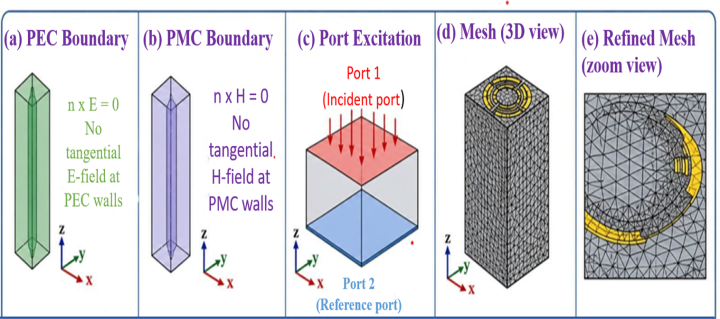
To rigorously solve the frequency-domain vector wave equation that dictates the spatial mapping of light-matter interactions, precise boundary conditions, waveguide ports, and localized mesh refinement strategies were enforced. Perfect electric conductor (PEC) was assigned along parallel walls perpendicular to the electric field vector by enforcing:
 | (5) |
Similarly, perfect magnetic conductor (PMC) was enforced on the orthogonal pair of lateral boundaries to establish a perfect magnetic wall 12, 13:
 | (6) |
The vector wave equation is solved via 14:
 | (7) |
where  is the electric field vector,
  is the free-space wave number, and
  relative permittivity of the material.
Port 1 (Incident Port) launches a normally incident wave along the negative z-direction, while Port 2 (Reference Port) captures transmitted power. Scattering parameters are gathered to compute macroscopic optical coefficients (R, T, and A).
To link these macroscopic results to quantum state modulation, the Local Density of Optical States (LDOS), ρ(r, ω), which determines the emission decay rate of a quantum emitter via the Purcell effect as seen by 15, is evaluated directly from the green's tensor of the classical electric field enhancement:
 | (8) |
where  is the free-space LDOS, and Gsc is the scattered green's tensor, proportional to our calculated local electric field norm |E|. A global 3D unstructured tetrahedral mesh discretizes the volume (Figure 2).

The full-wave numerical modeling of the graphene-based planar metamaterial is governed by the specific geometric, thermodynamic, and material constants detailed in Table
We demonstrated the active control of light-matter interactions and quantum emitter environments by evaluating the spectral absorptance (A) across a frequency range from 0.1 to 6.0 THz as a function of graphene's Fermi energy Ef. As illustrated in Figure 3, modulating Ef from 0.05 eV to 0.6 eV reveals a highly tunable behavior transitioning from weak light-matter coupling to near-perfect critical coupling, which agrees with 16.
At low levels, graphene behaves like a lossy dielectric with low carrier concentration. For Ef = 0.05 eV, light-matter coupling remains weak, and absorptance stays below 13% across the entire band. At Ef = 0.1 eV, a broad resonance begins to appear near 2.2 THz, peaking at 23%. At Ef = 0.2 eV, a stable resonant profile forms with a peak absorptance of 52% at 2.85 THz. At Ef = 0.5 eV, the system reaches a near-perfect absorption peak of approximately 98% at 4.3 THz due to the critical coupling condition, matching trends in hybrid architectures.
A continuous blueshift of the resonance peak frequency is observed as Ef increases. By varying the gate voltage to tune Ef, the resonance frequency shifts dynamically across a wide bandwidth from 2.2 THz to 4.3 THz. This features a dynamic mechanism to tune the metamaterial to match specific quantum emitter emission frequencies.

function of incident frequency (THz) for varying graphene Fermi energy levels
(Ef = 0.05 eV to 0.6 eV).
At low levels, graphene behaves like a lossy dielectric with low carrier concentration. For Ef = 0.05 eV, absorptance remains below 13% across the entire band. At Ef = 0.1eV, a broad resonance begins to appear near 2.2 THz peaking at 23%. At Ef = 0.2 eV, a resonant profile form with a peak absorptance of 52% at 2.85 THz. At Ef = 0.5 eV, the system reaches a near-perfect absorption peak of approximately 98% at 4.3 THz due to the critical coupling condition which is similar to what was gotten by 16.
A continuous blueshift of the resonance peak frequency is observed as Ef increases. By varying the gate voltage to tune Ef, the resonance frequency shifts dynamically across a wide bandwidth from 2.2 THz to 4.3THz. In summary, when Ef increases, intra-band transitions dominate the surface conductivity.
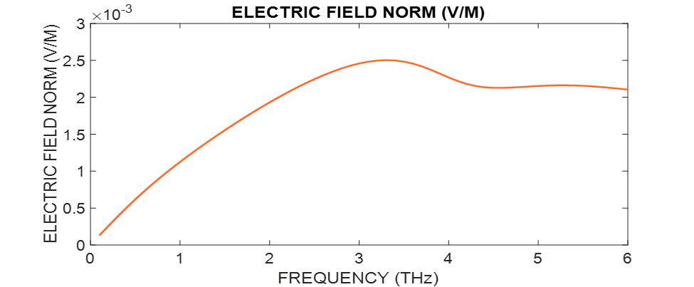
We investigated how the metamaterial enhances high-precision light-matter interactions; the global integrated electric field norm was tracked as a function of frequency. As shown in Figure 4, the electric field amplitude exhibits a clear resonant peak.
The curve rises steadily from near-zero up to a maximum localized value at approximately 3.3 THz. This peak marks the global localized surface plasmon resonance of the structural array, which agrees with 13. Beyond 3.3 THz, the field profile encounters a slight dip and settles into a plateau around 4.5 to 6.0 THz, mapping the system's transition into higher-order multi-polar regimes. This pronounced spectral field enhancement provides the physical mechanism required to increase the local density of optical states (LDOS), delivering the high-precision coupling needed to manipulate and route localized quantum states.

The curve rises steadily from near-zero up to a maximum localized value at approximately 3.3 THz. This peak marks the global localized surface plasmon resonance of the structural array which is in agreement with 17. Beyond 3.3 THz, the field profile encounters a slight dip and settles into a plateau around 4.5 to 6 THz, mapping the system's transition into higher-order multi-polar regimes similar to results by 18. This pronounced spectral field enhancement provides the physical mechanism required to increase the local density of optical states (LDOS), delivering the high-precision coupling needed to manipulate quantum emitters as seen by 19.
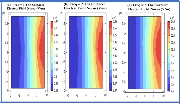
3.3. Spatial Electromagnetic Field DistributionTo unveil the microscopic origins of this quantum state control, 2D spatial profiles of the surface electric field norm were mapped at different frequencies across the band.
At 1 THz, the field maximum is limited to 4.97 x 10⁶ V/m, representing a weak light-matter interaction regime. At 3 THz, aligning with the strong resonance slope, the field is amplified significantly to 14.5 x 10⁶ V/m, localizing intensely along the right structural boundary and establishing a spatial gradient for asymmetric quantum state interactions.
At 1 THz as shown in Figure 5a, the field maximum is limited to 4.97 x 10⁶ V/m. At 3 THz in Figure 5c, aligning with the strong resonance slope, the field is amplified significantly to 14.5 x 10⁶ V/m, localizing intensely along the right structural boundary.

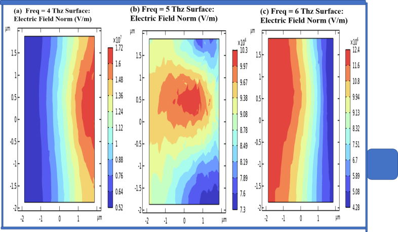
The peak field intensity reaches its absolute maximum of 1.72 x 10⁷ V/m at 4 THz, matching the near-perfect absorption threshold under high gate voltage conditions. This maximum spatial field confinement creates a deep subwavelength hot-zone that drastically enhances the Purcell factor, enabling strong coupling between the metamaterial and local quantum states. The same trend is also observed in the research by 20.
At 5 THz, the edge-localized gradient transforms into a central oval hotspot (x = 0 um) peaking at 1.03 x 10⁷ V/m, indicating a higher-order symmetric mode similar to results by Jahangiri et al. At 6 THz, the field layout flips completely to the left boundary (x = -2 um) at 1.24 x 10⁷ V/m due to an out-of-phase scattering regime. This complete spatial mode inversion demonstrates that a quantum emitter's decay pathway can be dynamically routed to different spatial channels depending on the excitation frequency 21; as shown in Figure 6:

A comparative summary of the near-field performance parameters across the simulated spectrum is organized in Table 3.
This work has presented a robust computational modeling framework to engineer strong light-matter interactions using a graphene-integrated planar metamaterial. By employing a transition boundary condition and solving the frequency-domain vector wave equation under exact PEC and PMC conditions, we successfully evaluated both macroscopic optical properties and localized quantum field environments. The platform demonstrates near-perfect absorption of 98% and strong near-field confinement of 1.72 x 10⁷ V/m with a gate-tunable resonant blueshift from 2.2 THz to 4.3 THz. These dynamic spatial and spectral field transformations alter the local density of optical states (LDOS), offering an effective route for chip-scale quantum state generation, quantum emission control, and high-precision quantum optical circuits. Future work should focus on the fabrication and experimental characterization of the proposed planar metamaterial structures via THz time-domain spectroscopy (THz-TDS) to validate these design rules in physical quantum hardware environments.
| [1] | X. Heng et al., “Quantum-Enhanced Sensing with Squeezed Light: From Fundamentals to Applications,” Applied Sciences, vol. 15, no. 18, p. 10179, 2025. | ||
| In article | View Article | ||
| [2] | A. Farmani and A. Omidniaee, “FDTD-based design of high quality factor quantum dot photonic crystal nanolaser for next-generation nanotechnologies,” Scientific Reports, 2026. | ||
| In article | View Article PubMed | ||
| [3] | A. Scrivano, “Innovative approaches in cloud computing: Balancing efficiency, scalability, and sustainability,” Authorea Preprints, 2025. | ||
| In article | View Article | ||
| [4] | S. Wang et al., “Single-Substrate Circularly Polarized Huygens’ Metasurface With Independent Modulation of Electric and Magnetic Impedances,” IEEE Transactions on Microwave Theory and Techniques, vol. 73, no. 8, pp. 4658–4670, 2025. | ||
| In article | View Article | ||
| [5] | R. Méndez-Camacho, E. Cruz-Hernández, and M. López-López, “Field-tunable charge confinement in III–V layered nanowire-array superlattices,” Scientific Reports, 2026. | ||
| In article | View Article PubMed | ||
| [6] | T. Hime et al., “Solid-state qubits with current-controlled coupling,” science, vol. 314, no. 5804, pp. 1427–1429, 2006. | ||
| In article | View Article PubMed | ||
| [7] | Y.-H. Yu, X.-Y. Li, K. Xu, and H. Fan, “Mathieu Control of the Effective Coupling in Superconducting Qubits,” arXiv preprint arXiv: 2512.24992, 2025. | ||
| In article | |||
| [8] | S. Aghili, “Engineered Photonic Structures for Enhanced Light–Matter Interaction and Telecom-Band DFB Lasers,” 2026. | ||
| In article | |||
| [9] | J. Guo et al., “Shape Function-Based Eddy Current Approach for Thickness Measurement of Thermal Barrier Coatings,” IEEE Sensors Journal, vol. 26, no. 2, pp. 3172–3183, 2025. | ||
| In article | View Article | ||
| [10] | P. Rodriguez-Lopez, J.-S. Wang, and M. Antezza, “Electric conductivity in graphene: Kubo model versus a nonlocal quantum field theory model,” Physical Review B, vol. 111, no. 11, p. 115428, 2025. | ||
| In article | View Article | ||
| [11] | X. Fu, J. Yang, S. Wang, and P. Huo, “Bridging photocatalysis and plasmonics: the dual role of interband and intraband transitions,” Chemical Communications, vol. 62, no. 10, pp. 3167–3177, 2026. | ||
| In article | View Article PubMed | ||
| [12] | M. S. Anwar et al., “Confinement Driven Spin‐Texture Evolution in Directly Written Nanomagnets,” Advanced Functional Materials, vol. 35, no. 49, p. e13904, 2025. | ||
| In article | View Article | ||
| [13] | S.-H. Kim and C.-S. Kee, “Mirrorless open cavities enabled by boundary incompatibility between perfect electric conductor and perfect magnetic conductor parallel-plate waveguides,” Scientific Reports, vol. 16, no. 1, p. 14269, 2026. | ||
| In article | View Article PubMed | ||
| [14] | Y. Saifullah, H. Wang, C. Qian, and H. Chen, “Metamaterials for water waves: theory, design, and applications,” Advanced Functional Materials, vol. 36, no. 28, p. e21623, 2026. | ||
| In article | View Article | ||
| [15] | G. Huang et al., “Transfer and beyond: emerging strategies and trends in two-dimensional material device fabrication,” Chemical Society Reviews, 2026. | ||
| In article | |||
| [16] | M. N. Hamza et al., “Nanophotonic perfect absorber with ultra-broadband terahertz-to-infrared response via hybrid-material design for advanced optical sensing,” PloS one, vol. 21, no. 2, p. e0342168, 2026. | ||
| In article | View Article PubMed | ||
| [17] | M. P. Mcoyi, K. T. Mpofu, M. Sekhwama, and P. Mthunzi-Kufa, “Developments in localized surface plasmon resonance,” Plasmonics, vol. 20, no. 7, pp. 5481–5520, 2025. | ||
| In article | View Article | ||
| [18] | L.-H. Mo, R. Moessner, and H. Zhao, “Complex and tunable heating in conformal field theories with structured drives via classical ergodicity breaking,” Physical Review B, vol. 112, no. 18, p. 184304, 2025. | ||
| In article | View Article | ||
| [19] | W. Wen, J. Li, and Y. Liu, “Local and Nonlocal Pathways to Quantum Light with Quantum Photonic Materials,” Advanced Functional Materials, vol. 36, no. 39, p. e24326, 2026. | ||
| In article | View Article | ||
| [20] | M. Shahnewaz Shaid, M. Rezwan Ahmed, and M. Samiul Habib, “Switchable ultra-broadband to multi-frequency THz absorption in a VO2-graphene hybrid metamaterial,” Optical Materials Express, vol. 16, no. 3, pp. 507–527, 2026. | ||
| In article | View Article | ||
| [21] | M. Alotaibi, Y. Abughnheim, L. Al Sakkaf, and U. Al Khawaja, “Phase-controlled elastic, inelastic, and coalescent collisions of two-dimensional flat-top solitons,” Physical Review E, vol. 113, no. 5, p. 054202, 2026. | ||
| In article | View Article PubMed | ||
Published with license by Science and Education Publishing, Copyright © 2026 Cyrus Anuri Abiri, Kenneth K. Sirma, Jared O. Gwaro and Qasim M. Mehmood
 This work is licensed under a Creative Commons Attribution 4.0 International License. To view a copy of this license, visit
http://creativecommons.org/licenses/by/4.0/
This work is licensed under a Creative Commons Attribution 4.0 International License. To view a copy of this license, visit
http://creativecommons.org/licenses/by/4.0/
| [1] | X. Heng et al., “Quantum-Enhanced Sensing with Squeezed Light: From Fundamentals to Applications,” Applied Sciences, vol. 15, no. 18, p. 10179, 2025. | ||
| In article | View Article | ||
| [2] | A. Farmani and A. Omidniaee, “FDTD-based design of high quality factor quantum dot photonic crystal nanolaser for next-generation nanotechnologies,” Scientific Reports, 2026. | ||
| In article | View Article PubMed | ||
| [3] | A. Scrivano, “Innovative approaches in cloud computing: Balancing efficiency, scalability, and sustainability,” Authorea Preprints, 2025. | ||
| In article | View Article | ||
| [4] | S. Wang et al., “Single-Substrate Circularly Polarized Huygens’ Metasurface With Independent Modulation of Electric and Magnetic Impedances,” IEEE Transactions on Microwave Theory and Techniques, vol. 73, no. 8, pp. 4658–4670, 2025. | ||
| In article | View Article | ||
| [5] | R. Méndez-Camacho, E. Cruz-Hernández, and M. López-López, “Field-tunable charge confinement in III–V layered nanowire-array superlattices,” Scientific Reports, 2026. | ||
| In article | View Article PubMed | ||
| [6] | T. Hime et al., “Solid-state qubits with current-controlled coupling,” science, vol. 314, no. 5804, pp. 1427–1429, 2006. | ||
| In article | View Article PubMed | ||
| [7] | Y.-H. Yu, X.-Y. Li, K. Xu, and H. Fan, “Mathieu Control of the Effective Coupling in Superconducting Qubits,” arXiv preprint arXiv: 2512.24992, 2025. | ||
| In article | |||
| [8] | S. Aghili, “Engineered Photonic Structures for Enhanced Light–Matter Interaction and Telecom-Band DFB Lasers,” 2026. | ||
| In article | |||
| [9] | J. Guo et al., “Shape Function-Based Eddy Current Approach for Thickness Measurement of Thermal Barrier Coatings,” IEEE Sensors Journal, vol. 26, no. 2, pp. 3172–3183, 2025. | ||
| In article | View Article | ||
| [10] | P. Rodriguez-Lopez, J.-S. Wang, and M. Antezza, “Electric conductivity in graphene: Kubo model versus a nonlocal quantum field theory model,” Physical Review B, vol. 111, no. 11, p. 115428, 2025. | ||
| In article | View Article | ||
| [11] | X. Fu, J. Yang, S. Wang, and P. Huo, “Bridging photocatalysis and plasmonics: the dual role of interband and intraband transitions,” Chemical Communications, vol. 62, no. 10, pp. 3167–3177, 2026. | ||
| In article | View Article PubMed | ||
| [12] | M. S. Anwar et al., “Confinement Driven Spin‐Texture Evolution in Directly Written Nanomagnets,” Advanced Functional Materials, vol. 35, no. 49, p. e13904, 2025. | ||
| In article | View Article | ||
| [13] | S.-H. Kim and C.-S. Kee, “Mirrorless open cavities enabled by boundary incompatibility between perfect electric conductor and perfect magnetic conductor parallel-plate waveguides,” Scientific Reports, vol. 16, no. 1, p. 14269, 2026. | ||
| In article | View Article PubMed | ||
| [14] | Y. Saifullah, H. Wang, C. Qian, and H. Chen, “Metamaterials for water waves: theory, design, and applications,” Advanced Functional Materials, vol. 36, no. 28, p. e21623, 2026. | ||
| In article | View Article | ||
| [15] | G. Huang et al., “Transfer and beyond: emerging strategies and trends in two-dimensional material device fabrication,” Chemical Society Reviews, 2026. | ||
| In article | |||
| [16] | M. N. Hamza et al., “Nanophotonic perfect absorber with ultra-broadband terahertz-to-infrared response via hybrid-material design for advanced optical sensing,” PloS one, vol. 21, no. 2, p. e0342168, 2026. | ||
| In article | View Article PubMed | ||
| [17] | M. P. Mcoyi, K. T. Mpofu, M. Sekhwama, and P. Mthunzi-Kufa, “Developments in localized surface plasmon resonance,” Plasmonics, vol. 20, no. 7, pp. 5481–5520, 2025. | ||
| In article | View Article | ||
| [18] | L.-H. Mo, R. Moessner, and H. Zhao, “Complex and tunable heating in conformal field theories with structured drives via classical ergodicity breaking,” Physical Review B, vol. 112, no. 18, p. 184304, 2025. | ||
| In article | View Article | ||
| [19] | W. Wen, J. Li, and Y. Liu, “Local and Nonlocal Pathways to Quantum Light with Quantum Photonic Materials,” Advanced Functional Materials, vol. 36, no. 39, p. e24326, 2026. | ||
| In article | View Article | ||
| [20] | M. Shahnewaz Shaid, M. Rezwan Ahmed, and M. Samiul Habib, “Switchable ultra-broadband to multi-frequency THz absorption in a VO2-graphene hybrid metamaterial,” Optical Materials Express, vol. 16, no. 3, pp. 507–527, 2026. | ||
| In article | View Article | ||
| [21] | M. Alotaibi, Y. Abughnheim, L. Al Sakkaf, and U. Al Khawaja, “Phase-controlled elastic, inelastic, and coalescent collisions of two-dimensional flat-top solitons,” Physical Review E, vol. 113, no. 5, p. 054202, 2026. | ||
| In article | View Article PubMed | ||